
Ceramic Quad Flat Package - Cerquad
Application:
CQFPs are hermetic multilayer packages with square and rectangular body frames. The package leads are brazed on the top or bottom of the package with design options to meet a variety of applications.
Material:
• Flexibility of surface-mount board level assembly or socketing
• EIAJ or JEDEC configurations
• Lead Plating: Gold, Solder Dip, or Tin
Features:
• Lead counts for small and high pin count configurations
• Lead pitch from 15.7 mils to 50 mils
• Lead form: Flat, Gull Wing, J-Bend
Hybrid Package - Multi-Chip Module (MCM)
Application:
A Hybrid Package is a special carrier of hybrid microcircuits and components interconnected as one unit. It can be considered a component of an electronic subsystem.
Materials:
The Hybrid may consist of a single construction or be made up of sub-modules. Each module usually contains a compartment to house the hermetically packaged hybrids and discrete passive component parts such as transformers, axle-lead resistors, etc.
These packages come in a wide variety of package configurations; Ceramic, Metal, DIP style and Flat Pack.
Features:
- Wide variety of package configurations and lead counts
- Packages available in metal, DIP style, Flat Pack
- Hermetic
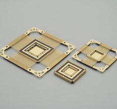
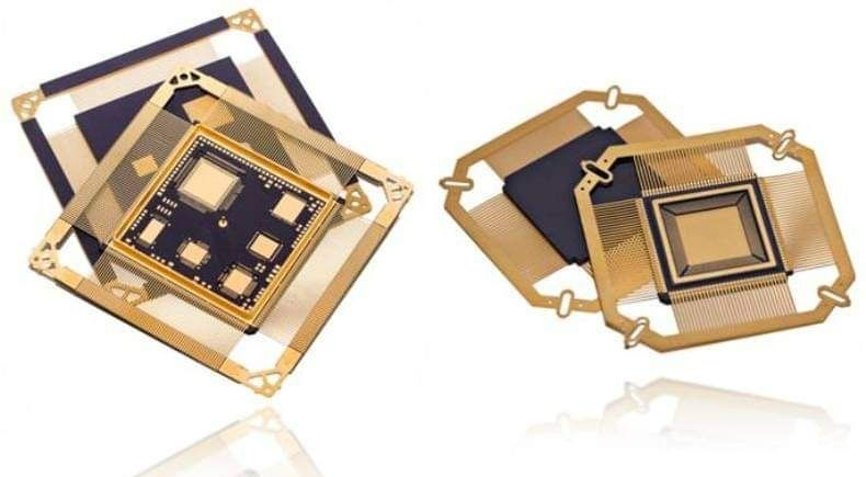
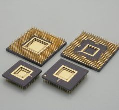
Leaded Chip Carrier (LDCC) / Flat Pack
Flat Packs have small body outlines and are lightweight. They usually have leads on two sides of the package parallel to the seating plane. Lead counts range from 10-224. The lead spacing depends on the package but ranges from .015-.050 inches.
QFP's or JLDCC's are typically found with leads greater than 24 on all four sides of the ceramic body. These packages are hermetically sealed and are used for surface mount applications. They can be soldered directly to a PC Board or used in a socket. The lead spacing depending on the package can come in .015, .020, .025 and .050 inches.
Features:
- Hermeticity
- Leads allow package to expand/contract without placing undue stress on the package to PCB connection
- Available in Flat, Gullwing or J Lead configurations

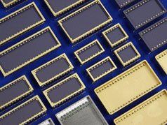
Leadless Chip Carrier (LCC)
Application
LCC Packages offer thermal performance in high heat dissipation applications. The package is able to expand and contract during heating and cooling cycles minimizing undue stress on the package to PCB connection.
LCC packages are square or rectangular surface-mount ceramic package that has no leads. For electrical connection the LCC instead uses flat metal contacts (or metallized castellations) known as pads around the four sides of the package bottom.
LCC’s have pad counts that range from 8 to 100 with the pad pitch (distance between pads) typically either 50 mils or 40 mils. Leadless Chip Carriers are a good option for surface mount applications. The LCC can either be directly soldered onto the PCB or operated using a socket.
Material
Both HTCC and LTCC materials are available. Please refer to the material properties of the table with respect to material properties.
Features:
• Multilayer Ceramic Package
• Two or four side, Top Brazed option
• Excellent electrical performance and thermal management
• Footprint Compatible with J Leaded and PLCC
• Surface Mount or Socket Applications
• Gold Plated Leads
• Solder, Glass or Epoxy Seal
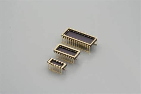
Side-Braze Packages (DIP)
Application:
Dual in-line packages with conventional thru-hole and J-bend lead configurations. The standard Sidebraze package, commonly known as a "DIP", consists of two rows of leads brazed onto the sides of the ceramic. The row spacing varies from leadcount, but can come in .300, .400, .600 and .900 inch wide configurations.
The DIP is extremely popular due to its reliability and ease of use. As the lead count increases, the package size increases sharply thereby reducing the space efficiency. As the lead count increases, the internal lead traces also increase. This will increase the electrical characteristics of the package.
Features:
- High performance and reliability
- Ease of PC board mounting via socket, manual or automated equipment
- Ease of soldering and reliable removal techniques
- Lead spacing matches common PC Board layouts and allow one or more leads to run between the PC Board holes
- Effective heat dissipation
- Seal using solder, glass or epoxy
- Pin counts range 8-64 leads
- EIAJ or JEDEC configurations
PGA (Pin Grid Array)
Application
The PGA, is a square or rectangular through-hole ceramic package with pins arranged in a square array at the bottom of the package body. PGA’s are a popular choice for devices due to high I/O signal carrying capacity, excellent electrical performance and high thermal heat dissipation all with minimal package size. Typical PGA’s have pin counts ranging from 28-476 and pins are usually spaced 100 mils (approximately 2.54 mm) apart.
Material
HTCC materials are available.
Features:
- Excellent electrical performance in a wide range of package sizes
- Small through hole mounting package with rugged construction
- High I/O signal carrying capacity
- Hermetically encapsulated packages offering enhanced thermal dissipation
- Multilayer Ceramic Package
- Footprint Compatible with PPGA
- Through Hole or Socket Mount
- Solder, Glass or Epoxy Seal
- Cavity Up or Cavity Down Configuration
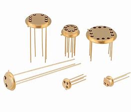
Transistor Outlines (TO Headers)
TO Headers are intended for high reliability miniature microcircuit applications. The single piece construction provides great strength and resistance to stress. The absence of sidewalls helps to facilitate circuit installation, as well as inspection and test accessibility.
We can offer a wide range of sizes and lead counts. Our TO Headers are standard so they’ll meet most any requirement.
Features:
- High Reliability
- Single piece construction
- Easy accessibility for circuit installation, testing and inspection due to no sidewall
- Low cost metal cans are available with solder or seam seal options.

Power Transistor Outline (TO) Packages
The Power transistor Outline (TO) Package is a type of “transistor outline” package that features a metallic body with two flat metal tabs which enable it to dissipate large amounts of heat. TO packages are hermetically sealed to protect the device from environmental factors such as contaminants and moisture. The leads protrude from the bottom of the package through glass and ceramic feed-throughs that insulate them from the metal body. These packages are mostly used for transistors, thyristors, and integrated circuits with low lead counts such as voltage regulators that are intended for high-reliability and mission-critical circuits. The metal tabs perform as heat sinks themselves, but they each have a hole so that they can easily be screwed onto a larger heat sink if higher power handling capability is required. The tabs are located on opposite corners of the back of the body.
Advantages of Power Transistor Outline (TO) Packages
Used for packaging high-power and high voltage devices
Excellent thermal properties from Cu/W heat sinks than can include BeO and ALN inserts
Packages meet Military and Space specifications
Open tooled designs such as TO254, TO257 and TO258
Full Hermiticity 1×10⁻⁸
Metal seal ring for seam sealing